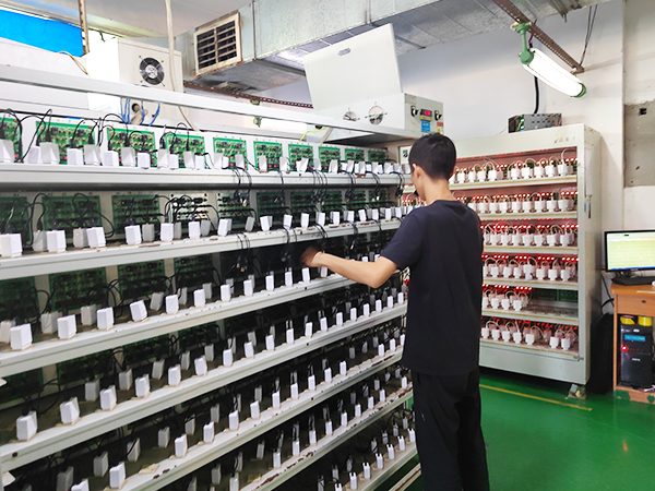
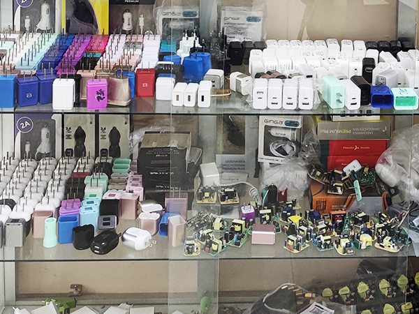
Power adapter manufacturers Saiyue Technology Co., Ltd., more than 10 years of focus on power supply R & D manufacturing, quality assurance! Power adapter manufacturers, today to introduce you to the appearance of switching power supply to pay attention to those matters, appearance inspection is mainly analysis to check the appearance of switching power supply products defects, the purpose of the appearance inspection is to record the physical dimensions, materials, design, structure and marking of PCB, electronic parts and solder joints, etc., to determine the appearance of the breakage, detection of contamination and other abnormalities and defects, these problems are caused by process manufacturing or application of Evidence of errors, overloads and operational errors, information that is likely to be correlated with failure.
Visual inspection is usually used for exterior inspection, but a 1.5 to 10x magnification or optical microscope may also be used. One of the roles of the appearance inspection is to verify the process failure of the PCB, electronic parts and solder joints with the standards and specifications of the consistency; appearance inspection of the role of the second is to find the problem points that may lead to failure. For example, power adapter, charger assembly of finished products placed after a period of time shell cracks, it may be PC / ABS two raw materials resin compatibility is not handled well, easy to crack, or process, the product processing process, not well eliminate internal stress. If there is a foreign object between the outer leads, the foreign object may lead to a short circuit between the leads. mechanical damage to the surface of the PCB may lead to PCB alignment fracture caused by open circuit, etc.
In addition, special attention should be paid to the following aspects of the content of the inspection:
1. mechanical damage: from the electronic parts of the pins, roots and packaging sealing seam cracks, scratches, blemishes; solder joints and mechanical damage to the PCB surface traces.
2. Device sealing defects: from the electronic components of the pin and the combination of glass, ceramic and plastic, as well as the root of the adhesion parts and sealing seams.
3. Device pin plating defects: uneven plating, bubbles, pinholes and rust spots from the surface of electronic components.
4. PCB surface contamination or adhesion: mainly from the PCB board processing process.
6. PCB delamination and bursting, etc.
7. PCB surface treatment layer of the abnormal.
8. Solder joints have not occurred remelting and cracking, false welding, etc.
 SaiYue Technology talks about the rumors of mobile phone charging
 What is the use of the bluetooth adapter? Many people do not know
 How to use and maintain mobile phone chargers
 Can a 65w charger charge a 33w phone?